Apple IIe Motherboard: Difference between revisions
(Created page with "Image:IMG_20200206_085701304_HDR-Store-tiny.png|thumb|Apple IIe "Rev B" Motherboard, Current Version|link=https://wiki.reactivemicro.com/images/3/33/IMG_20200206_085701304_H...") |
Tag: Manual revert |
||
| (17 intermediate revisions by the same user not shown) | |||
| Line 14: | Line 14: | ||
==Kit Assembly== | ==Kit Assembly== | ||
The Apple IIe Motherboard Kit is a total of | The Apple IIe Motherboard Kit is a total of 1517 pads or "''solder joints''". It takes about 3 hours to fully assemble a kit if you have a decent iron, flux, and solder. The parts included with your kit and the PCB have basic labels. Those with intermediate knowledge should have little trouble assembling the kit from the labels on the parts, the bag, and the PCB. The images below of the motherboards can also be used for reference or to determine orientation, such as the diodes. | ||
| Line 20: | Line 20: | ||
* Start with the small passive parts like caps and resistors. Some of the location labels will be hard to see if you start with the sockets or other parts. Each time a part is added you can simply bend over a leg on each side to help hold the part to the PCB which allows the board to be turned over and prevents parts from falling out. It is most simple to load all the parts in groups and then solder and clip the legs as needed. | * Start with the small passive parts like caps and resistors. Some of the location labels will be hard to see if you start with the sockets or other parts. Each time a part is added you can simply bend over a leg on each side to help hold the part to the PCB which allows the board to be turned over and prevents parts from falling out. It is most simple to load all the parts in groups and then solder and clip the legs as needed. | ||
* '''A good loupe (magnifying glass) is recommended for helping identify and confirm parts, like the markings on some small caps. It also helps with solder joint inspection. An illuminated 40 x 25mm and a 35 x 50mm loupe are well worth the investment and can be had for about $10 each on eBay.''' | |||
Your kit | |||
===Resistors=== | |||
Your kit includes resistors. They should be the less precise "4 band" style which are typically 5% tolerance. You can also use the more precise "5 band" style which are typically 1% tolerance. Here are some charts on how to read them to help make matching locations on your PCB more easy. | |||
| Line 27: | Line 30: | ||
File:4_Band_Resistor_Chart.svg|4-band Resistor Markings|link=https://wiki.reactivemicro.com/images/8/85/4_Band_Resistor_Chart.svg | File:4_Band_Resistor_Chart.svg|4-band Resistor Markings|link=https://wiki.reactivemicro.com/images/8/85/4_Band_Resistor_Chart.svg | ||
File:5_Band_Resistor_Chart.svg|5-band Resistor Markings|link=https://wiki.reactivemicro.com/images/2/29/5_Band_Resistor_Chart.svg | File:5_Band_Resistor_Chart.svg|5-band Resistor Markings|link=https://wiki.reactivemicro.com/images/2/29/5_Band_Resistor_Chart.svg | ||
File:Resistornetwork.jpg|Resistor Network Markings, "Pin1" Dot Left|link=https://wiki.reactivemicro.com/images/c/c6/Resistornetwork.jpg | |||
</gallery> | </gallery> | ||
| Line 36: | Line 40: | ||
! scope="col"| Value | ! scope="col"| Value | ||
|- | |- | ||
! scope="row"| | ! scope="row"| R30,R37-38,R73 | ||
| | | 47 ohms | ||
|- | |- | ||
! scope="row"| | ! scope="row"| R1 | ||
| | | 56 ohms | ||
|- | |- | ||
! scope="row"| | ! scope="row"| R8,R40 | ||
| | | 75 ohms | ||
|- | |||
! scope="row"| R16* | |||
| 75 ohms (2 watts) | |||
|- | |- | ||
! scope="row"| | ! scope="row"| R9,R17,R21-24 | ||
| 100 ohms | | 100 ohms | ||
|- | |- | ||
! scope="row"| | ! scope="row"| R41-44 | ||
| 120 ohms | |||
|- | |||
! scope="row"| R34-35 | |||
| 150 ohms | | 150 ohms | ||
|- | |- | ||
! scope="row"| | ! scope="row"| R11,R45 | ||
| 200 ohms | |||
|- | |||
! scope="row"| R36 | |||
| 270 ohms | |||
|- | |||
! scope="row"| R5 | |||
| 330 ohms | | 330 ohms | ||
|- | |- | ||
! scope="row"| | ! scope="row"| R15,R19,R25,R27-R29 | ||
| 1k ohms | | 1k ohms | ||
|- | |- | ||
! scope="row"| R7 | ! scope="row"| R7 | ||
| | | 2.7k ohms | ||
|- | |- | ||
! scope="row"| | ! scope="row"| R10 | ||
| | | 5.6k ohms | ||
|- | |- | ||
! scope="row"| | ! scope="row"| R3,R13 | ||
| | | 6.8k ohms | ||
|- | |- | ||
! scope="row"| | ! scope="row"| R4,R6,R12,R14,R20 | ||
| 12k ohms | | 12k ohms | ||
|- | |- | ||
! scope="row"| | ! scope="row"| R39 | ||
| 47k ohms | | 47k ohms | ||
|- | |- | ||
! scope="row"| | ! scope="row"| R32 | ||
| 100k ohms | |||
|- | |||
! scope="row"| R18 | |||
| 1M ohms | | 1M ohms | ||
|- | |- | ||
! scope="row"| | ! scope="row"| *Can be omitted if RM PSU is used. | ||
|- | |- | ||
|} | |} | ||
</center> | </center> | ||
Related to the resistors are the Resistor Network Arrays. These are the SIP (single inline pin) parts for locations RP1-RP3. Each has a 'dot' on the part and PCB to determine Pin1, which are all toward the keyboard end of the PCB. | |||
===Capacitors & Didoes=== | |||
<gallery class="center" widths=400px heights=250px caption="Example illustrations of different caps, a diode, and their related markings"> | |||
File:Caps_Chart.svg|Caps Markings|link=https://wiki.reactivemicro.com/images/d/d1/Caps_Chart.svg | |||
File:Diode_Anatomy.svg|Diode Markings|link=https://wiki.reactivemicro.com/images/e/e9/Diode_Anatomy.svg | |||
</gallery> | |||
'''Note: '''Cautionary care needs to be taken while installing capacitors and diodes.<br/> | |||
If your kit includes Aluminum or Tantalum capacitors, or "caps" for short, then be sure to install them in the correct orientation. The PCB will be clearly marked with "+" signs for all cap locations when the orientation of the part matters, or a polarized part is normally used. Sometimes a non-polarized part is used in place of a polarized one and then its orientation does not matter, however install a polarized cap backwards and you will damage it. An Aluminum Electrolytic will have a strip pointing to the NEGATIVE end lead. A Tantalum Electrolytic will generally have a marking or stripe to denote (not always pointing to) the POSITIVE lead. | |||
<center> | |||
{| class="wikitable" style="text-align: center; | |||
!colspan="20" style="font-size: 100%;" | <font color="blue">Here is a list of capacitors on the PCB:</font> | |||
|- | |||
! scope="col"| PCB Location | |||
! scope="col"| Value | |||
|- | |||
! scope="row"| C34-35,C37,C40,C71 | |||
| 22nF, Ceramic Cap | |||
|- | |||
! scope="row"| C1-7,10-11,13,16,18-24,26-31,33 | |||
| 100nf, Ceramic Cap | |||
|- | |||
! scope="row"| 37-39,41-52,55-69,73-76,78-81,83-89 | |||
| 100nf, Ceramic Cap | |||
|- | |||
! scope="row"| C70 | |||
| 47pF, Ceramic Cap | |||
|- | |||
! scope="row"| C32 | |||
| 47pF, Mica Cap | |||
|- | |||
! scope="row"| C25 | |||
| 100pF, Ceramic Cap | |||
|- | |||
! scope="row"| C90-93 | |||
| 220pF, Ceramic Cap | |||
|- | |||
! scope="row"| C9,C8,C12,C15,C17,C53-54,C72,C82 | |||
| 10uF, Electrolytic Cap | |||
|- | |||
! scope="row"| CR4 | |||
| Diode | |||
|- | |||
! scope="row"| CR1, CR2 | |||
| LED, Red | |||
|- | |||
|} | |||
</center> | |||
* Install the Aluminum caps and be sure to install correctly as they are polarized. | |||
* All caps will have value markings on them. "106" is 10uF, and "104" is .1uF. 10uF is also typically physically larger than .1uF. "470" is 47pF, "101" is 100pF, and "221" is 220pF for example. This should also help identify the ceramic caps in the kit. They along with the Electrolytic caps can also clearly be seen in the assembled pic above. | |||
* Be sure to installed the LEDs correctly. One side of the base of the LED will be "flat" compared to the other side. Be sure to align the flat side as noted on the motherboard location marking. This same rule will apply to the transistors as well. | |||
===IC Sockets=== | |||
* Once the passive parts are installed next should be the IC sockets. When a socket is loaded on the board bending the corner pins of the sockets helps hole it to the PCB which allows group loading and soldering. The sockets are all the same thickness. So if you solder on a flat surface then this will also help hold all the sockets flat to the PCB and give a more uniform appearance when completed. '''Be sure ALL pin 1 'notches' '''are facing towards the keyboard end. The CPU socket 'notch' should be towards the Game IO / Video side, and the ROM SPCL should be facing towards the crystal side. | * Once the passive parts are installed next should be the IC sockets. When a socket is loaded on the board bending the corner pins of the sockets helps hole it to the PCB which allows group loading and soldering. The sockets are all the same thickness. So if you solder on a flat surface then this will also help hold all the sockets flat to the PCB and give a more uniform appearance when completed. '''Be sure ALL pin 1 'notches' '''are facing towards the keyboard end. The CPU socket 'notch' should be towards the Game IO / Video side, and the ROM SPCL should be facing towards the crystal side. | ||
* End with the larger parts, like jacks, and finally the slots. Don't bend over these parts pins/legs as they will be too hard. You will need to hold them in place as you solder a few pins before you can group solder. | * End with the larger parts, like jacks, and finally the slots. Don't bend over these parts pins/legs as they will be too hard. You will need to hold them in place as you solder a few pins before you can group solder. | ||
Latest revision as of 11:10, 17 October 2022

The Apple IIe Motherboard project was started on August 12th, 2022 by Henry from ReActiveMicro, and was officially released on , 2022.
This marks the second full computer project released by ReActiveMicro, the first being the Apple II Plus Rev 7 RFI. The concept is a replacement board which is known good and fully tested, to be used as a replacement for the original motherboard.
Product Status: Actively sold by ReActiveMicro.
Support: Post on the Discussion page (link above) or email ReActiveMicro Support.
Sales: Visit the ReActiveMicro Store.
Kit Assembly
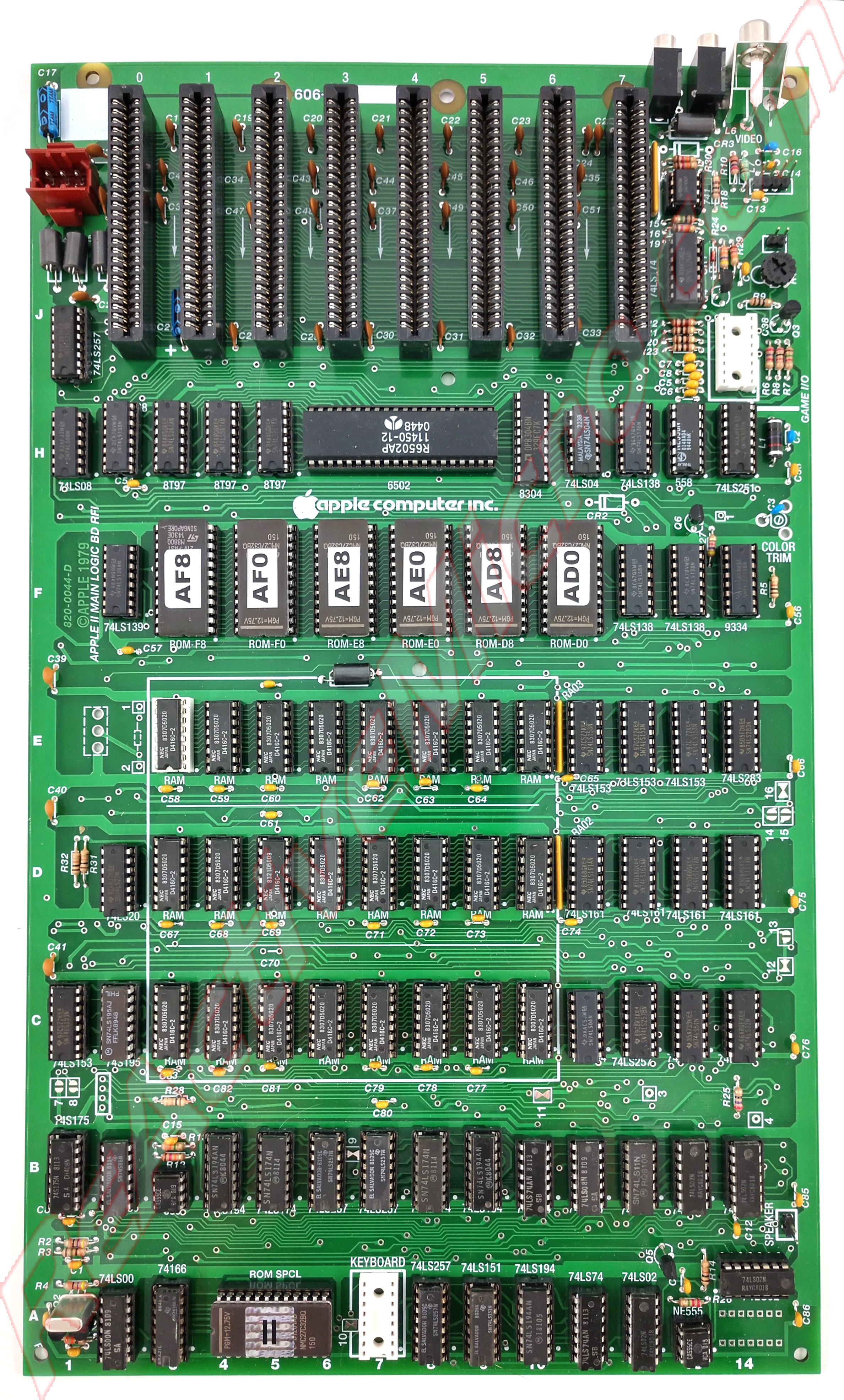
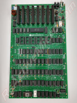
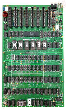
The Apple IIe Motherboard Kit is a total of 1517 pads or "solder joints". It takes about 3 hours to fully assemble a kit if you have a decent iron, flux, and solder. The parts included with your kit and the PCB have basic labels. Those with intermediate knowledge should have little trouble assembling the kit from the labels on the parts, the bag, and the PCB. The images below of the motherboards can also be used for reference or to determine orientation, such as the diodes.
To assemble your kit we recommend adding parts in groups and then soldering them. This will be the fastest way to assemble the PCB rather than adding one part at a time then soldering it.
- Start with the small passive parts like caps and resistors. Some of the location labels will be hard to see if you start with the sockets or other parts. Each time a part is added you can simply bend over a leg on each side to help hold the part to the PCB which allows the board to be turned over and prevents parts from falling out. It is most simple to load all the parts in groups and then solder and clip the legs as needed.
- A good loupe (magnifying glass) is recommended for helping identify and confirm parts, like the markings on some small caps. It also helps with solder joint inspection. An illuminated 40 x 25mm and a 35 x 50mm loupe are well worth the investment and can be had for about $10 each on eBay.
Resistors
Your kit includes resistors. They should be the less precise "4 band" style which are typically 5% tolerance. You can also use the more precise "5 band" style which are typically 1% tolerance. Here are some charts on how to read them to help make matching locations on your PCB more easy.
-

4-band Resistor Markings
-

5-band Resistor Markings
-

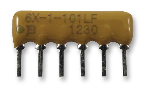
Resistor Network Markings, "Pin1" Dot Left


| Here is a list of resistors on the PCB: | |||||||||||||||||||
|---|---|---|---|---|---|---|---|---|---|---|---|---|---|---|---|---|---|---|---|
| PCB Location | Value | ||||||||||||||||||
| R30,R37-38,R73 | 47 ohms | ||||||||||||||||||
| R1 | 56 ohms | ||||||||||||||||||
| R8,R40 | 75 ohms | ||||||||||||||||||
| R16* | 75 ohms (2 watts) | ||||||||||||||||||
| R9,R17,R21-24 | 100 ohms | ||||||||||||||||||
| R41-44 | 120 ohms | ||||||||||||||||||
| R34-35 | 150 ohms | ||||||||||||||||||
| R11,R45 | 200 ohms | ||||||||||||||||||
| R36 | 270 ohms | ||||||||||||||||||
| R5 | 330 ohms | ||||||||||||||||||
| R15,R19,R25,R27-R29 | 1k ohms | ||||||||||||||||||
| R7 | 2.7k ohms | ||||||||||||||||||
| R10 | 5.6k ohms | ||||||||||||||||||
| R3,R13 | 6.8k ohms | ||||||||||||||||||
| R4,R6,R12,R14,R20 | 12k ohms | ||||||||||||||||||
| R39 | 47k ohms | ||||||||||||||||||
| R32 | 100k ohms | ||||||||||||||||||
| R18 | 1M ohms | ||||||||||||||||||
| *Can be omitted if RM PSU is used. | |||||||||||||||||||
Related to the resistors are the Resistor Network Arrays. These are the SIP (single inline pin) parts for locations RP1-RP3. Each has a 'dot' on the part and PCB to determine Pin1, which are all toward the keyboard end of the PCB.
Capacitors & Didoes
- Example illustrations of different caps, a diode, and their related markings
-

Caps Markings
-

Diode Markings


Note: Cautionary care needs to be taken while installing capacitors and diodes.
If your kit includes Aluminum or Tantalum capacitors, or "caps" for short, then be sure to install them in the correct orientation. The PCB will be clearly marked with "+" signs for all cap locations when the orientation of the part matters, or a polarized part is normally used. Sometimes a non-polarized part is used in place of a polarized one and then its orientation does not matter, however install a polarized cap backwards and you will damage it. An Aluminum Electrolytic will have a strip pointing to the NEGATIVE end lead. A Tantalum Electrolytic will generally have a marking or stripe to denote (not always pointing to) the POSITIVE lead.
| Here is a list of capacitors on the PCB: | |||||||||||||||||||
|---|---|---|---|---|---|---|---|---|---|---|---|---|---|---|---|---|---|---|---|
| PCB Location | Value | ||||||||||||||||||
| C34-35,C37,C40,C71 | 22nF, Ceramic Cap | ||||||||||||||||||
| C1-7,10-11,13,16,18-24,26-31,33 | 100nf, Ceramic Cap | ||||||||||||||||||
| 37-39,41-52,55-69,73-76,78-81,83-89 | 100nf, Ceramic Cap | ||||||||||||||||||
| C70 | 47pF, Ceramic Cap | ||||||||||||||||||
| C32 | 47pF, Mica Cap | ||||||||||||||||||
| C25 | 100pF, Ceramic Cap | ||||||||||||||||||
| C90-93 | 220pF, Ceramic Cap | ||||||||||||||||||
| C9,C8,C12,C15,C17,C53-54,C72,C82 | 10uF, Electrolytic Cap | ||||||||||||||||||
| CR4 | Diode | ||||||||||||||||||
| CR1, CR2 | LED, Red | ||||||||||||||||||
- Install the Aluminum caps and be sure to install correctly as they are polarized.
- All caps will have value markings on them. "106" is 10uF, and "104" is .1uF. 10uF is also typically physically larger than .1uF. "470" is 47pF, "101" is 100pF, and "221" is 220pF for example. This should also help identify the ceramic caps in the kit. They along with the Electrolytic caps can also clearly be seen in the assembled pic above.
- Be sure to installed the LEDs correctly. One side of the base of the LED will be "flat" compared to the other side. Be sure to align the flat side as noted on the motherboard location marking. This same rule will apply to the transistors as well.
IC Sockets
- Once the passive parts are installed next should be the IC sockets. When a socket is loaded on the board bending the corner pins of the sockets helps hole it to the PCB which allows group loading and soldering. The sockets are all the same thickness. So if you solder on a flat surface then this will also help hold all the sockets flat to the PCB and give a more uniform appearance when completed. Be sure ALL pin 1 'notches' are facing towards the keyboard end. The CPU socket 'notch' should be towards the Game IO / Video side, and the ROM SPCL should be facing towards the crystal side.
- End with the larger parts, like jacks, and finally the slots. Don't bend over these parts pins/legs as they will be too hard. You will need to hold them in place as you solder a few pins before you can group solder.
-
93-Series ROM
-
27-Series ROM