Apple II Plus Rev 7 RFI: Difference between revisions
Created page with "==Kit Assembly== To do: Add note for RAs. Each has a 'dot' on the part and PCB to determine Pin1. RA01 has the Pin1 towards the slots. RA02 and RA03 have Pin1 towards the keyb..." |
|||
| Line 1: | Line 1: | ||
==Kit Assembly== | ==Kit Assembly== | ||
To do: Add note for RAs. Each has a 'dot' on the part and PCB to determine Pin1. RA01 has the Pin1 towards the slots. RA02 and RA03 have Pin1 towards the keyboard. RA01 has the silk screen border around all pads for the part. RA02 and RA03 has the silk screen border around only the inner 6 pads. Pin1 and Pin8 are outside the boarder. | To do: | ||
Add note for RAs. Each has a 'dot' on the part and PCB to determine Pin1. RA01 has the Pin1 towards the slots. RA02 and RA03 have Pin1 towards the keyboard. RA01 has the silk screen border around all pads for the part. RA02 and RA03 has the silk screen border around only the inner 6 pads. Pin1 and Pin8 are outside the boarder. | |||
Mention "A good loupe is recommended for helping identify and confirm parts, like the markings on some small caps. It also helps with soldering inspection. An illuminated 40 x 25mm and a 35 x 50mm loupe are well worth the investment and can be had for under $10 each on eBay. | |||
--------------------------------------------------------------------------------------------------------- | --------------------------------------------------------------------------------------------------------- | ||
Revision as of 12:14, 30 June 2019
Kit Assembly
To do: Add note for RAs. Each has a 'dot' on the part and PCB to determine Pin1. RA01 has the Pin1 towards the slots. RA02 and RA03 have Pin1 towards the keyboard. RA01 has the silk screen border around all pads for the part. RA02 and RA03 has the silk screen border around only the inner 6 pads. Pin1 and Pin8 are outside the boarder.
Mention "A good loupe is recommended for helping identify and confirm parts, like the markings on some small caps. It also helps with soldering inspection. An illuminated 40 x 25mm and a 35 x 50mm loupe are well worth the investment and can be had for under $10 each on eBay.
The parts included with your v1.0 kit and the PCB have basic labels. There are 2153 pads which need to be soldered. Those with intermediate knowledge should have little trouble assembling the kit from the labels on the parts, the bag, and the PCB. The images of the motherboard can also be used for reference or determine orientation, such as the diodes.
Some care does need to be taken when installing capacitors and diodes however.
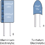
If your kit includes Aluminum or Tantalum capacitors, or "caps" for short, then be sure to install them in the correct orientation. The PCB will be clearly marked with "+" signs for all cap locations when the orientation of the part matters, or a polarized part is normally used. Sometimes a non-polarized part is used in place of a polarized one and then its orientation does not matter. However install a polarized cap backwards and you will damage it. An Aluminum Electrolytic will have a strip pointing to the NEGATIVE end lead. A Tantalum Electrolytic will generally have a marking or stripe to denote (not always pointing to) the POSITIVE lead.
All caps will have value markings on them. "106" is 10uF, and "104" is .1uF. 10uF is also physically a lot larger than .1uF. This should help identify the two ceramic caps in the kit. They along with the Electrolytic caps can also clearly be seen in the assembled pic above.
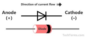
A diode also has a marking on it, and needs to be installed correctly as it only allows current to flow in one direction. Install it backwards and you won't usually damage it, however the circuit will no longer operate as intended. They can also clearly be seen in the assembled pic above.
- Here is an example pic of different caps, a diode, and their related markings.
-
Caps Markings
-
Diode Markings
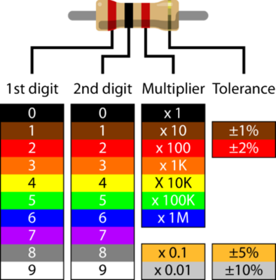
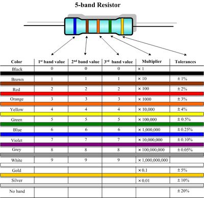
Your kit may include resistors. If so they could be the less precise "4 band" style which are typically 5% tolerance. Or the more precise "4 band" style which are typically 1% tolerance. Here are some charts on how to read them to help make matching locations on your PCB more easy.
-
4-band Resistor Markings
-
5-band Resistor Markings


