Apple IIe Motherboard

The Apple IIe Motherboard project was started on August 12th, 2022 by Henry from ReActiveMicro, and was officially released on , 2022.
This marks the second full computer project released by ReActiveMicro, the first being the Apple II Plus Rev 7 RFI. The concept is a replacement board which is known good and fully tested, to be used as a replacement for the original motherboard.
Product Status: Actively sold by ReActiveMicro.
Support: Post on the Discussion page (link above) or email ReActiveMicro Support.
Sales: Visit the ReActiveMicro Store.
Kit Assembly
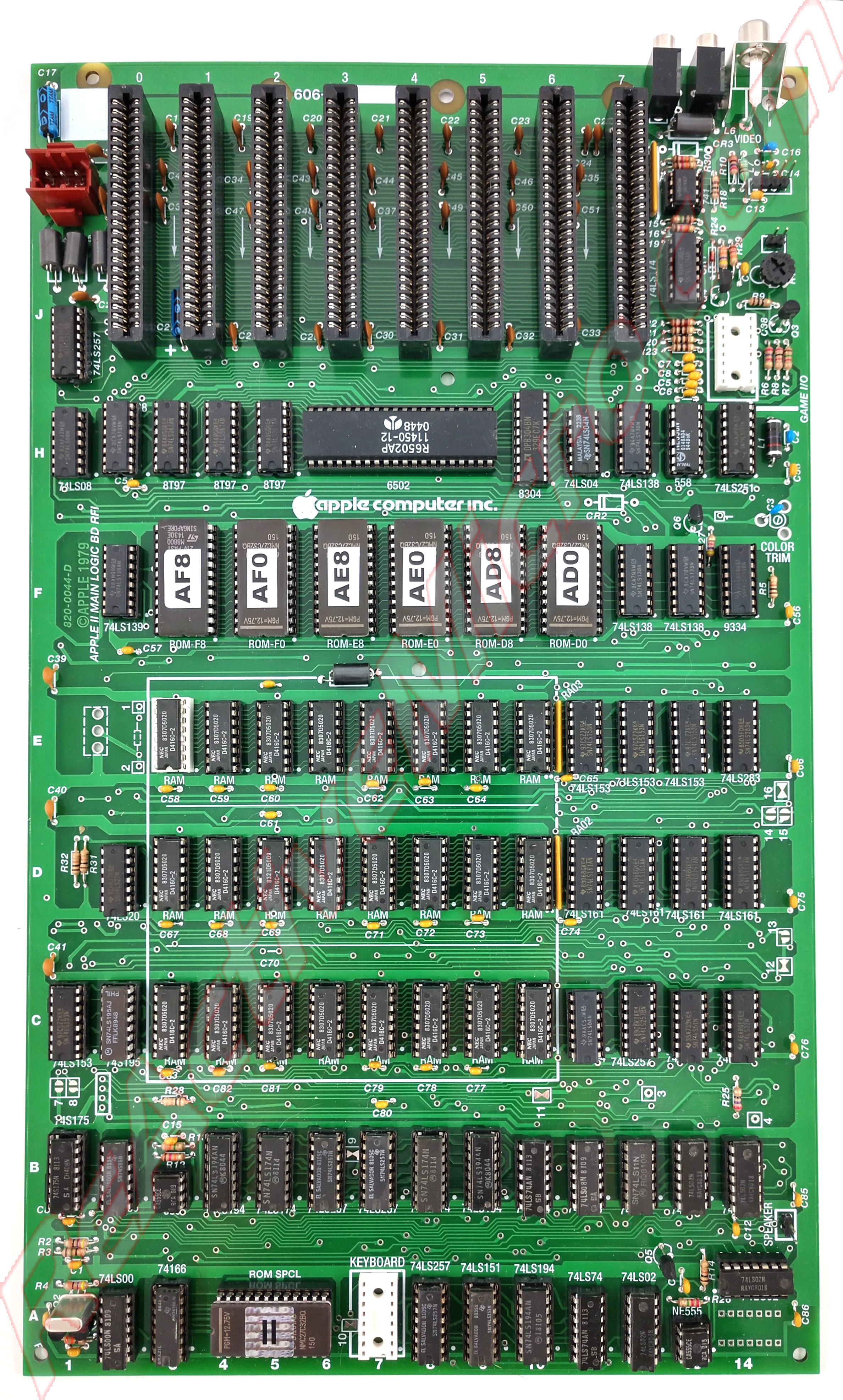
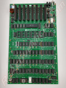
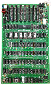
The Apple IIe Motherboard Kit is a total of 1515 pads or "solder joints". It takes about 3 hours to fully assemble a kit if you have a decent iron, flux, and solder. The parts included with your kit and the PCB have basic labels. Those with intermediate knowledge should have little trouble assembling the kit from the labels on the parts, the bag, and the PCB. The images below of the motherboards can also be used for reference or to determine orientation, such as the diodes.
To assemble your kit we recommend adding parts in groups and then soldering them. This will be the fastest way to assemble the PCB rather than adding one part at a time then soldering it.
- Start with the small passive parts like caps and resistors. Some of the location labels will be hard to see if you start with the sockets or other parts. Each time a part is added you can simply bend over a leg on each side to help hold the part to the PCB which allows the board to be turned over and prevents parts from falling out. It is most simple to load all the parts in groups and then solder and clip the legs as needed.
Your kit also includes resistors. They should be the less precise "4 band" style which are typically 5% tolerance. You can also use the more precise "5 band" style which are typically 1% tolerance. Here are some charts on how to read them to help make matching locations on your PCB more easy.
-

4-band Resistor Markings
-

5-band Resistor Markings


| Here is a list of resistors on the PCB: | |||||||||||||||||||
|---|---|---|---|---|---|---|---|---|---|---|---|---|---|---|---|---|---|---|---|
| PCB Location | Value | ||||||||||||||||||
| R9 | 10 ohms | ||||||||||||||||||
| R10, R25 | 27 ohms | ||||||||||||||||||
| R2, R4 | 47 ohms | ||||||||||||||||||
| R18, R20-23 | 100 ohms | ||||||||||||||||||
| R3 | 150 ohms | ||||||||||||||||||
| A1 | 330 ohms | ||||||||||||||||||
| R5, R14, R28, R31-32 | 1k ohms | ||||||||||||||||||
| R7 | 1.5k ohms | ||||||||||||||||||
| R8 | 2k ohms | ||||||||||||||||||
| R6 | 2.7k ohms | ||||||||||||||||||
| R27 | 4.7k ohms | ||||||||||||||||||
| R12, R16-17,R19,R29-30 | 12k ohms | ||||||||||||||||||
| R24 | 47k ohms | ||||||||||||||||||
| R15 | 1M ohms | ||||||||||||||||||
| R26 | 2.2M ohms | ||||||||||||||||||
| R13 | 3.3M ohms | ||||||||||||||||||
Related to the resistors are the Resistor Network Arrays. These are the SIP (single inline pin) parts for RA01-RA03. Each has a 'dot' on the part and PCB to determine Pin1.
- RA01 has the Pin1 towards the REAR of the PCB (slot end).
- RA02 and RA03 have Pin1 toward the keyboard end.
- RA01 has the silk screen border around all pads for the part. RA02 and RA03 has the silk screen border around only the inner 6 pads. Pin1 and Pin8 are outside the boarder.
R30,R38,R47,R73 47 ohms, Resistor, .25w, 5%, 2.30x6mm
R1 56 ohms, Resistor, .25w, 5%, 2.3x6mm
R8,R40 75 ohms, Resistor, .25w, 5%, 2.3x6mm
R16 75 ohm, Resistor, 2w, 5%, 4.5 x 11.5mm
R9,R17,R21-24 100 ohms, Resistor, .25w, 5%, 2.3x6mm
R41-44 120 ohms, Resistor, .25w, 5%, 2.3x6mm
R35 150 ohms, Resistor, .25w, 5%, 2.30x6mm
R11,R45 200 ohms, Resistor, .25w, 5%, 2.3x6mm
R36 270 ohms, Resistor, .25w, 5%, 2.30x6mm
R5 330 ohms, Resistor, .25w, 5%, 2.30x6mm
R15,R19,R25,R27-R29 1k, Resistor, .25w, 5%, 2.3x6mm
R7 2.7k, Resistor, .25w, 5%, 2.30x6mm
R10 5.6k, Resistor, .25w, 5%, 2.3x6mm
R3,R13 6.8k, Resistor, .25w, 5%, 2.3x6mm
R4,R6,R12,R14,R20 12k, Resistor, .25w, 5%, 2.30x6mm
R39 47k, Resistor, .25w, 5%, 2.30x6mm
R32 100k, Resistor, .25w, 5%, 2.30x6mm
R18 1M, Resistor, .25w, 5%, 2.30x6mm
- Once the passive parts are installed next should be the IC sockets. When a socket is loaded on the board bending the corner pins of the sockets helps hole it to the PCB which allows group loading and soldering. The sockets are all the same thickness. So if you solder on a flat surface then this will also help hold all the sockets flat to the PCB and give a more uniform appearance when completed. Be sure ALL pin 1 'notches' are facing towards the keyboard end. The CPU socket 'notch' should be towards the Game IO / Video side, and the ROM SPCL should be facing towards the crystal side.
- End with the larger parts, like jacks, and finally the slots. Don't bend over these parts pins/legs as they will be too hard. You will need to hold them in place as you solder a few pins before you can group solder.
A good loupe (magnifying glass) is recommended for helping identify and confirm parts, like the markings on some small caps. It also helps with solder joint inspection. An illuminated 40 x 25mm and a 35 x 50mm loupe are well worth the investment and can be had for about $10 each on eBay.
-
93-Series ROM
-
27-Series ROM